
单壁碳纳米管网络的构建及其应用
发表时间:2022-11-02
背景介绍
本文介绍了一种先进的自组装方法,用于在各种基板上制造可调节的微纳米级SWCNT网络[12-14]。其次,作者展示了这些有组织的架构的集成,以应用于通过创建高度可控的SWCNT和硅基异质结来实现光电器件。这代表了一种新型的基于光电二极管的逻辑器件,它可以由光和电两种输入控制,具有高电压可切换光电流响应性(>1 A/W),光电压响应性(>105 V/W),以及良好的电和光开关比(电:>105和光:>104)[15]。第三,作者还通过用2,2,6,6-四甲基哌啶-官能化证明了这些SWCNT 网络用于高性能硫化氢(H2S)检测1-oxyl(TEMPO)[16]。最后,介绍了SWCNT网络的结构转化到连续的多壁碳纳米管,然后到石墨/多层石墨烯纳米带结构,使用一种新开发的电压控制方法,称为“纳米管聚变”,这不仅证明了工程碳纳米管的sp2结构新方法,而且大大提高了其电和热输运性能[17]。
单壁碳纳米管组装
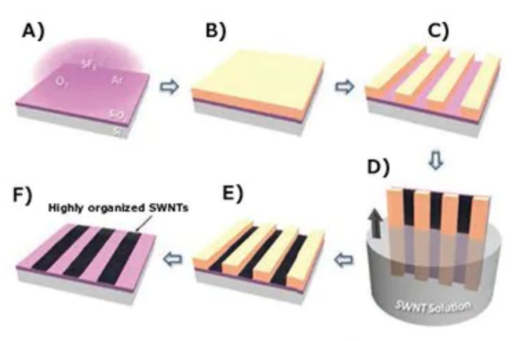
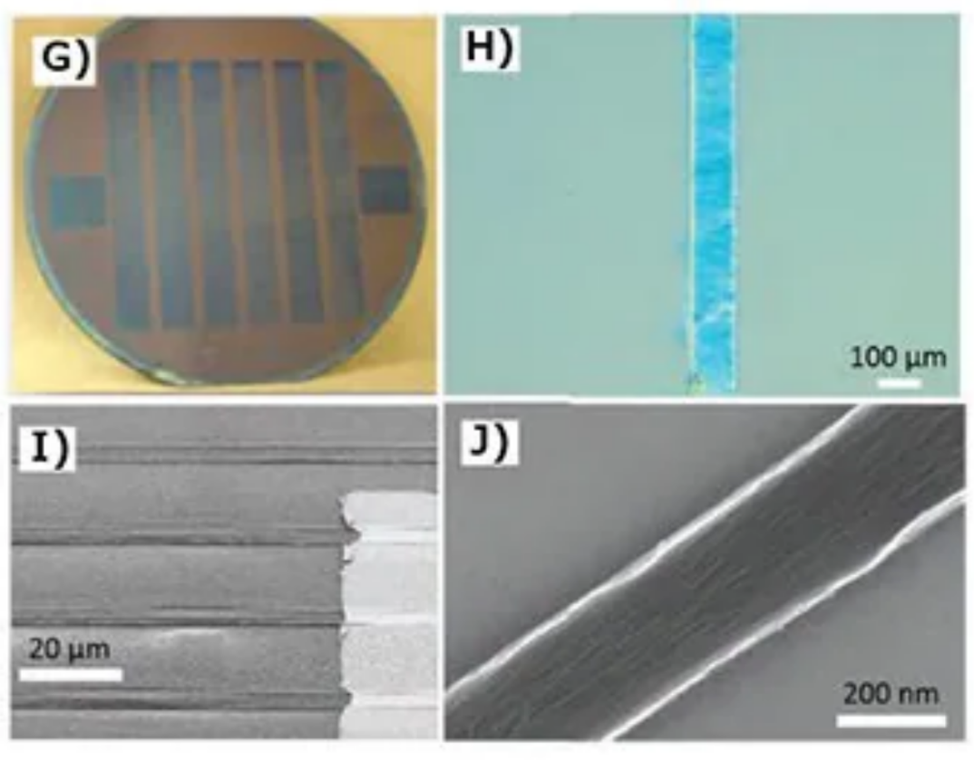
作者使用模板导向流体组件的方法来制备高度组织和对齐的SWCNTs薄膜,它采用了光刻图案模板辅助浸渍涂层[12–14],[18]。SWCNTs在预先设计的光刻胶通道之间直接组装在亲水性表面上,形成微和纳米尺度的高起源SWCNTs侧网络。等离子体处理可以提高流体组装的质量,增加悬浮键和表面亲水氢氧根官能团的数量。图1显示了模板引导射流组装方法的详细程序。图1A-C显示了SiO2基板经过等离子体处理,然后用光刻胶旋涂,并通过光刻技术(分别用于微纳米级图案的光刻和电子束光刻)进行图案化。图1D展示了使用浸涂机将预先图案化的基板首先垂直浸入SWCNT去离子(DI)水溶液中,然后以恒定的拉速度逐渐从溶液中提起的过程。图1E和1C显示了在去除光刻胶后,在SiO2衬底上的微/纳米级沟槽和SWCNT网络之间形成的SWCNT网络图案。图1G-J显示了SiO2/Si衬底上的厘米级、毫米级、微米级和纳米级组装的SWCNT网络。
基于光电应用的SWCNTS和Si异质结
开发基于硅的光子电路组件,例如片上源、调制器、存储等,是解决传统硅电路传输速度和集成度瓶颈的有希望的方法[19,20]。在这里,作者展示了SWCNT和硅的高度集成和控制异质结可以展示一个完全非常规的、急剧非线性的、反偏相关的光电流。这种新现象为获得高开关比的多功能模拟和混合数字光电运算提供了新的途径。可以通过电压的微小变化获得大的光电流切换,从而使光电门/器件具有逻辑输出,具体取决于光学和电子输入的逻辑状态。我们在厘米尺度的晶圆上展示了许多新型光电开关/器件和大量SWCNT架构器件的光刻组装。图2A和2E显示了高密度SWCNT/Si异质结图案的示意图和数字照片。SWCNTs通过模板流体法和常规光刻法在轻掺杂p的硅表面组装为微/纳米级器件结构,如图2F所示。图2B显示了SWCNT-Si结的暗和亮I-V曲线,以及具有相似尺寸的金属硅结中的光电流响应。虽然SWCNT-Si结中的暗I-V遵循传统二极管整流行为,但电流明显偏离了传统行为,即在反偏压Vr的几伏内急剧上升几个数量级,这与相同光源下同等尺寸的传统金属-Si肖特基结的发光I-V不同。提出的这些异质结能带结构的半定量模型表明,急剧的非线性光电流行为可能与SWCNT带中可用状态的反向偏置可调总数n(ε=eVr)有关。图2C展示了SWCNT组件Si传感器阵列的照片。图2G显示了连接到源极和漏极电极的叉指型SWCNT网络,这相当于两个背靠背光电二极管形成一个双向光电晶体管。图2H显示了一个混合输入的光电和门,光和施加的电压是输入,测量的电流是输出。此外,图2I-J分别显示了2位和4位数字光输入、电压可切换模拟输出加法器电路;当施加反向电压时,输出显示数字和的模拟等效值。因此,SWCNT-Si结是光电传感器、光转换器、光度测量和成像等光电应用的通用平台。
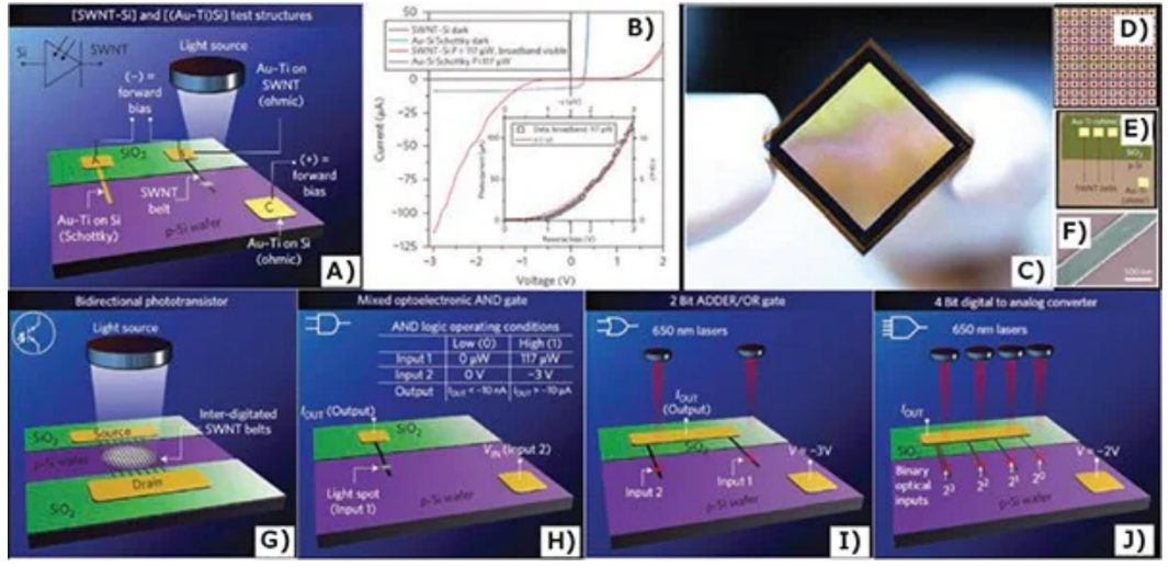
图2 新型光电器件示意图和SWCNT-Si传感器阵列图像 A)带有电极的 SWCNT-Si异质结测试结构(2cm×2cm);B)典型SWCNT-Si异质结的暗和亮I-V 曲线;C)SWCNT-Si传感器:0.25兆像素SWCNT-Si传感器阵列的数码照片(阵列面积,12mm×12mm)和D)传感器“核心”的SEM图像;E)SWCNT-Si异质结结构的数码照片;F)组装的SWCNT带SEM 图像;G)使用连接到源漏引线的叉指型SWCNT指的双向光电晶体管。该器件的有源区面积为3mm×200mm;H)具有光和电输入以及电输出的与门。结的有源区面积为3mm×100mm,插图:一组典型的工作条件,确定输入和输出条件的“低”和“高”逻辑状态;I)具有2个光学输入和一个电气输入和输出的2位加法器/或门;J)4位数模转换器
带SWCNT器件的高性能H2S检测器
SWCNT具有独特的纳米结构、高迁移率、高电流密度、高效电化学表面积等优点,是各种化学传感器积极研究的对象[8]。由于原始的基于CNT的化学传感器仅利用其固有的为了克服其在选择性和灵敏度方面的局限性,用共价或非共价材料对SWCNT进行功能化已被用于进一步提高基于SWCNT的化学传感器的灵敏度。需要注意的是,因为其一维纳米结构,SWCNT对湿度和周围温度等环境变化非常敏感。
在开发H2S气体传感器时,我们使用TEMPO分子掺杂作为SWCNT表面的催化剂,以提高室温下通过氧化还原反应检测H2S的灵敏度。图3A-D显示了高度组织的微传感器器件的SEM图像,这些器件通过模板导向流体组装方法,然后涂上TEMPO涂层,制备了大规模的SWCNT网络图案。图3E显示了用于功能化SWCNTs的TEMPO的化学结构。这种化合物能够氧化气态的H2S,可以用作H2S传感器的传感分子。图3F显示了功能化SWCNT传感器在不同浓度的H2S气体下的实时电流变化。图3G显示了器件的固有灵敏度和TEMPO功能化后的优势。另外,根据我们的结果,TEMPO可以被氧化为TEMPO+,这是H2S解离的一个非常重要的产物。TEMPO+到TEMPO-H的还原反应与H2S到S+2H++2e-的解离过程相耦合,因为在空气中,SWCNT器件由于氧离子(O2)的作用而表现出p型特性。新产生的电子被捐赠给SWCNT,使其不再具有P型特性,这使得功能化SWCNT比纯SWCNT更敏感。此外,我们发现湿度通过改善TEMPO到TEMPO+的变化来提高H2S的灵敏度。最后,本文还证明了用TEMPO功能化的SWCNT器件对随着湿度增加的H2S气体高度响应能力。半单壁碳纳米管尤其如此,它在60%的湿度下表现出高达420%的高灵敏度。
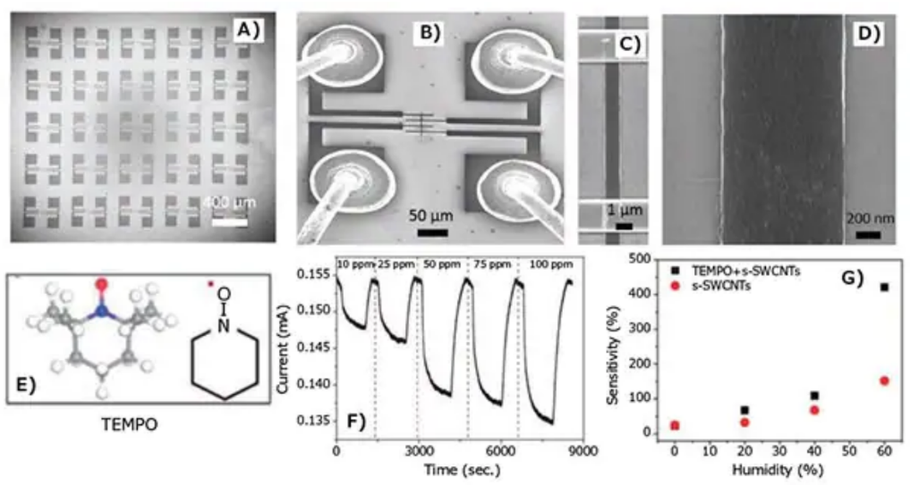
图3 基于SWCNT网络的高性能H2S检测器 A-D)组装好的SWCNT器件阵列的SEM图像;E)TEMPO分子的化学结构;F)功能化SWCNT传感器的实时电流随 H2S气体浓度的变化情况;G)无修饰的SWCNT器件和TEMPO功能化SWCNT器件的灵敏度随湿度的变化情况[16]。
SWCNT网络的电融合:同素异构体间转化
sp2结构碳纳米管的改性通常需要极端且难以控制的条件,例如高温、高压和高能辐照。本文提出了一种简单但功能强大的电学方法,通过施加受控的交流电压脉冲来实现碳纳米管从SWCNT到多壁碳纳米管(MWCNT)或多层石墨烯/石墨纳米带结构(MGNR)的结构转变。
通过控制电压脉冲的大小、源时间和应用于SWCNT网络的开关周期数,可以在不产生任何结构缺陷的情况下获得目标转化纳米结构(MWCNTs或GNRs)。另外还发现,经过结构改造后,SWCNT网络的电导率(高达35%的电阻降)和热导率(高达6-7倍的热导率,300 W/mK)都大大提高。图4A显示了在TEM网格上与金属电极组装的SWCNT网络结构。图4B显示了SWCNT网络的I-V 曲线、最大电流密度和击穿电压(Vb)。图4C显示了施加在SWCNT器件上的与时间相关的交流电压脉冲。图4D-F显示了电融合过程后原始SWCNT、MWNT(0.6Vb,3,000次循环)和GNR(0.8Vb,3,000次循环)的TEM图像。图4G-H显示了SWCNT器件在相同的3,000 次循环中在不同施加电压下的电阻变化和热导率。
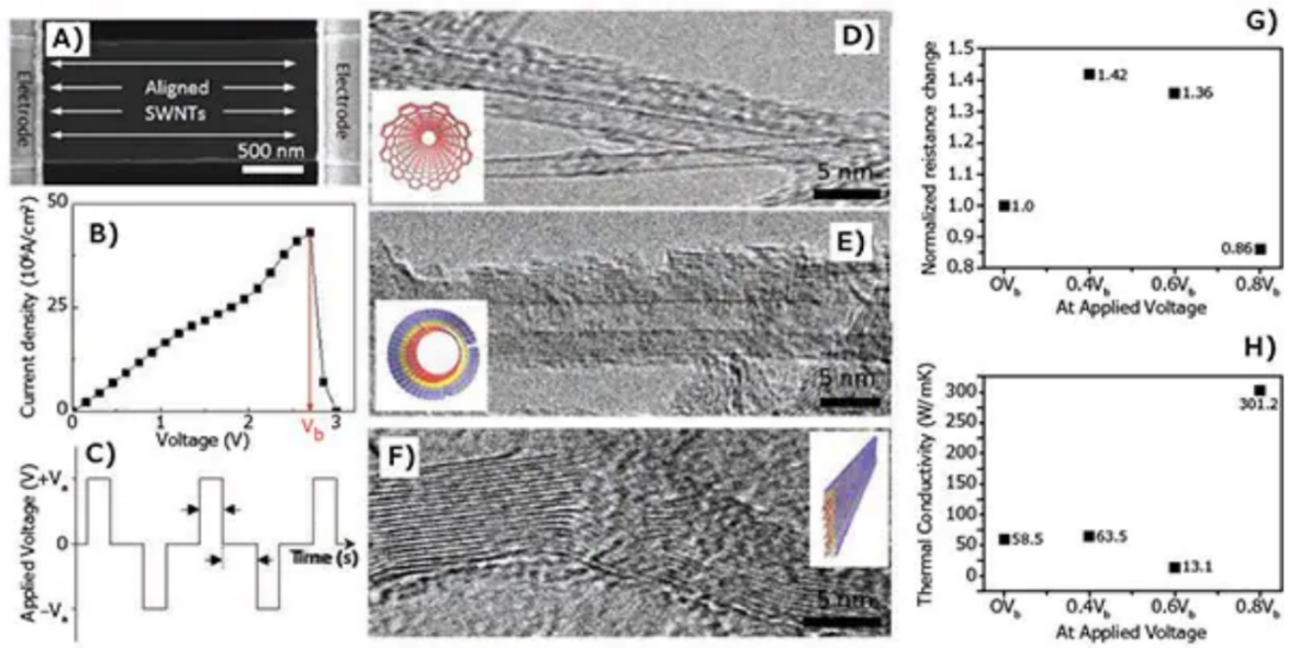
图4 脉冲交变电压诱导SWCNT的同素异构体转化及其电学和热学性能 A) 集成在特殊设计的TEM网格上的电极的组装SWCNT网络的SEM图像;B)显示电击穿行为的原始SWCNT网络设备的典型I-V特性,其中Vb是击穿电压;C)随时间变化的交流电压脉冲,用于SWCNT网络的结构转换;D)原始SWCNT的TEM图像;E)施加电压Va=0.6Vb,循环3000次后的多壁结构TEM图像; F)经Va=0.8Vb循环3000次后的多层石墨纳米带TEM图像;G-H)SWCNT网络在不同施加电压下 3,000次循环次数的电学和热学特性[17]。
结论
在这篇文章中,作者提出了一种高度组织SWCNT网络的模板引导流体组装方法。使用光刻图案化模板辅助浸涂,使用光刻图案模板辅助浸涂方法,SWCNTs直接组装在预先设计的微纳米级光刻胶通道之间,形成密集排列的、具有不同几何形状的SWCNTs侧网络,其特征尺寸从150纳米到数百微米尺度不等。这些高度组织的微纳米级SWCNT网络结构可以集成到各种传感器件架构中。模板导向流体装配技术的室温和晶圆级缩放兼容性提供了在大范围内可复制的可能性。在这方面,本文展示了一种高性能光电探测器和一种新型逻辑器件,基于SWCNT和硅的可扩展异质结,其输出电流可以完全由光和电输入控制。我们还介绍了一种基于SWCNT的化学传感器,该传感器可以通过使用TEMPO作为催化剂功能化的SWCNT网络上发生的氧化还原反应有效地检测H2S气体。
参考文献
1.Iijima S. 1991. Helical microtubules of graphitic carbon. Nature. 354(6348):56-58.
2.Avouris P. 2002. Molecular Electronics with Carbon Nanotubes. Acc. Chem. Res. 35(12):1026-1034.
3.Dai H. 2002. Carbon Nanotubes: Synthesis, Integration, and Properties. Acc. Chem. Res. 35(12):1035-1044.
4.Yao Z, Kane CL, Dekker C. High-Field Electrical Transport in Single-Wall Carbon Nanotubes. Phys. Rev. Lett. 84(13):2941-2944.
5.White CT, Todorov TN. 1998. Carbon nanotubes as long ballistic conductors. Nature. 393(6682):240-242.
6.Pop E, Mann D, Wang Q, Goodson K, Dai H. 2006. Thermal Conductance of an Individual Single-Wall Carbon Nanotube above Room Temperature. Nano Lett. 6(1):96-100.
7.Lu JP. 1997. Elastic properties of single and multilayered nanotubes. Journal of Physics and Chemistry of Solids. 58(11):1649-1652.
8.Kong J. 2000. Nanotube Molecular Wires as Chemical Sensors. 287(5453):622-625.
9.Wen L, Li F, Cheng H. 2016. Carbon Nanotubes and Graphene for Flexible Electrochemical Energy Storage: from Materials to Devices. Adv.Mater. 28(22):4306-4337.
10.Fan S. 1999. Self-Oriented Regular Arrays of Carbon Nanotubes and Their Field Emission Properties. 283(5401):512-514.
11.Shi Kam NW, O'Connell M, Wisdom JA, Dai H. 2005. Carbon nanotubes as multifunctional biological transporters and near-infrared agents for selective cancer cell destruction. Proceedings of the National Academy of Sciences. 102(33):11600-11605.
12.Jaber-Ansari L, Hahm MG, Somu S, Sanz YE, Busnaina A, Jung YJ. 2009. Mechanism of Very Large-Scale Assembly of SWNTs in Template Guided Fluidic Assembly Process. J. Am. Chem. Soc. 131(2):804-808.
13.Xiong X, Chen C, Ryan P, Busnaina AA, Jung YJ, Dokmeci MR. 2009. Directed assembly of high density single-walled carbon nanotube patterns on flexible polymer substrates. Nanotechnology. 20(29):295302.
14.Jaber-Ansari L, Hahm MG, Kim TH, Somu S, Busnaina A, Jung YJ. 2009. Large scale highly organized single-walled carbon nanotube networks for electrical devices. Appl. Phys. A. 96(2):373-377.
15.Kim YL, Jung HY, Park S, Li B, Liu F, Hao J, Kwon Y, Jung YJ, Kar S. 2014. Voltage-switchable photocurrents in single-walled carbon nanotube? silicon junctions for analog and digital optoelectronics. Nature Photon. 8(3):239-243.
16.Jung HY, Kim YL, Park S, Datar A, Lee H, Huang J, Somu S, Busnaina A, Jung YJ, Kwon Y. 2013. High-performance H2S detection by redox reactions in semiconducting carbon nanotube-based devices. Analyst. 138(23):7206.
17.Jung HY, Araujo PT, Kim YL, Jung SM, Jia X, Hong S, Ahn CW, Kong J, Dresselhaus MS, Kar S, et al. 2014. Sculpting carbon bonds for allotropic transformation through solid-state re-engineering of sp2 carbon. Nat Commun. 5(1):
18.Kim YL, Li B, An X, Hahm MG, Chen L, Washington M, Ajayan PM, Nayak SK, Busnaina A, Kar S, et al. 2009. Highly Aligned Scalable Platinum-Decorated Single-Wall Carbon Nanotube Arrays for Nanoscale Electrical Interconnects. ACS Nano. 3(9):2818-2826.
19.Almeida VR, Barrios CA, Panepucci RR, Lipson M. 2004. All-optical control of light on a silicon chip. Nature. 431(7012):1081-1084.
20.Liu L, Kumar R, Huybrechts K, Spuesens T, Roelkens G, Geluk E, de Vries T, Regreny P, Van Thourhout D, Baets R, et al. 2010. An ultra-small, low-power, all-optical flip-flop memory on a silicon chip. Nature Photon. 4(3):182-187.